0.13㎛ Technology
-
Technology Name
0.13㎛ CMOS Platform Technology
-
Overview
An 8-inch based 0.13㎛ CMOS platform technology provided as a fundamental technology for next-generation integrated technology.
-
Technical Features
The National Nanofab Center has established a 0.18㎛ CMOS platform technology and aims to develop an 8-inch based 0.13㎛ CMOS platform technology for the advancement to higher technology nodes. The 0.13㎛ CMOS platform technology can be implemented without significant new equipment investment and can be quickly built and provided faster than other technology nodes, satisfying the needs of technology demanders.
-
Technical Advantages
- The 0.13㎛ CMOS platform technology is a mature process technology that has been introduced to the market for a considerable amount of time, but it is still widely used in various product lines of commercial foundries developing many system semiconductors, making it a high-utility technology node.
- In domestic representative foundry product lines such as RF, Image Sensor, Mixed-Signal, IGBT, the 0.13㎛ CMOS platform can be used in a wide range of product lines, and it can be widely provided in fabless companies and companies that need foundries, with diverse applications.
- Also, it can be used as a fundamental technology for the development of fusion direct and single integration technologies, provided for new device convergence and device verification.
-
Application of
TechnologyIt can be expanded to business model commercialization strategies for various products used in the next-generation IT industries such as IoT, Automotive, and intelligent semiconductor markets that are attracting attention. By providing R&D process services to technology demanders (industry/academia/research), it is possible to build a flexible technology cooperation model among next-generation fabless-foundry. It is possible to configure a Selector with an underlying CMOS Transistor of an intelligent semiconductor.
-
Scope of Service and Technology Level
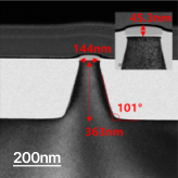
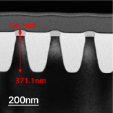
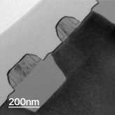
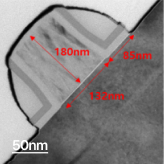
- Support for 200mm silicon-based 0.13㎛ CMOS technology service
- 1 Poly 5 Metal Process and MIM Capacito
- Core: 1.2V[N/PMOS] and IO: 3.3V[N/PMOS]
- Dual Gae Oxide and Poly-Si
- Spacer with Oxide/Nitride/Oxide structure
- Cobalt Silicide
- Wiring composed of Al and Ti/TiN Barrier
- USG and Low-K PMD layer configuration
-
Contact Information
Person in charge Lee Won-cheolContact 042-366-1614Email wc@nnfc.re.kr -
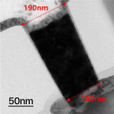
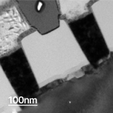
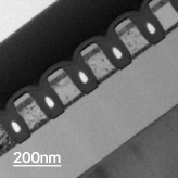
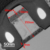
Related Images