Field
Thick MEMS
-
Technology Name
Thick MEMS process platform through Bulk Micromachining of Si substrate by DRIE process
-
Overview
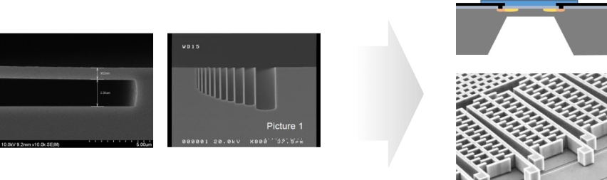
This is a process platform that can be applied to inertial, gas, and pressure sensors by fabricating high-aspect-ratio Si structures using Si, SOI, and SOG substrates.
-
Technical Features
- It is possible to fabricate sensors that can measure various physical and chemical properties through the backside etching of a Si substrate with a formed Membrane and electrode on top.
- Using SOI, SOG substrates with a certain thickness of Si sacrificial layer, it is possible to fabricate high-aspect-ratio Si structures and create sensors that can measure physical and chemical properties.
- The substrate and Membrane material, as well as the shape of the Si structure, can be freely modified.
-
Technical Advantages
- We provide 8-inch based process services, enabling the production of high productivity and various types of devices.
- Through single-crystal Si structures and highly uniform DRIE processes, reliable and high-yield sensor production is possible in MEMS device fabrication.
- Ultra-precision photolithography processes allow for the production of ultra-small devices.
-
Application of
Technology- MEMS Sensor through Si Backside Etching: Gas, Pressure Sensors, etc.
- MEMS Sensor using SOI, SOG Substrate: Inertial, Gas Sensors, etc.
-
Scope of Service and
Technology Level- 8" Si Backside DRIE: Membrane materials (SiOx, SiNx, etc.)
- SOI, SOG substrate DRIE: BOX, Si Film thickness is Customized
- Top CD : 100nm ~ 100um
- AR : 50:1
- ER :1~5um/min
-
Contact Information
Person in charge Joo-beom LeeContact 042-366-1571Email jblee@nnfc.re.kr -
Related Images