Field
Thin MEMS
-
Technology Name
AlN Thin Film-based MEMS Process Platform
-
Overview
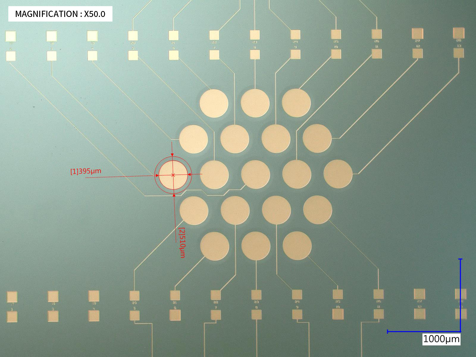
This is an ultrasonic transducer/resonator-based sensor platform utilizing the piezoelectric properties of C-axis oriented AlN thin films.
-
Technical Features
- -It is characterized by the use of seed layer deposition and Mo electrode for piezoelectric AlN crystallinity.
- To minimize the damage of AlN thin film during the process, TMAH is not used and 1 um AlN thin film patterning is performed using dry etching process.
- DRIE process is performed on the Silicon backside to generate resonance of the device.
-
Technical Advantages
- We provide 8-inch based process services, enabling high productivity and the fabrication of various types of devices.
- The high uniformity of AlN films and low residual stress (40>MPa) of 0.5% (1 sigma) allow for the production of MEMS devices with uniform performance.
- High crystallinity (Rocking curve FWHM less than 1.2 degrees) allows for high piezoelectric performance expectations.
-
Application of
Technology- MEMS Sensors: Ultrasonic imagers, ultrasonic distance sensors, ultrasonic gas sensors, bio sensors
- Thin film-based resonators/filters: Due to the high acoustic velocity of AlN, it can be used to manufacture FBAR and filters that can be used in 5G.
-
Scope of Service and
Technology LevelThe National Nanofab Center has the capability to provide AlN-based thin film MEMS process technology, and services can be provided at the following scope and technology level.
: Support for the development of 200 mm SOI WAFER-based thin film AlN MEMS start-up products -
Related Images