Field
WLP
-
Technology Name
Wafer Level Packaging
-
Overview
A platform that bonds wafers and wafers using heat and pressure, such as a wafer composed of sensor devices and a wafer for the purpose of protecting that sensor.
-
Technical Features
- Divided into methods using an intermediate medium and those that do not.
- Methods that do not use an intermediate medium include Anodic bonding, which bonds Glass and Silicon, and SDB (Silicon direct bonding), which directly bonds Silicon and Silicon.
- Methods using an intermediate medium are generally Thermal Compression bonding through heat and pressure, and include Glass Frit, Eutectic, Diffusion, and Adhesive methods.
-
Technical Advantages
- WLP (Wafer Level Packaging) is the process of packaging the wafer, a substrate used in semiconductor processes, in its current state.
- The purpose is to reduce the size and capacity by combining two or more chips in a wafer state, without attaching each packaged semiconductor chip to Ceramic, PCB, or any other substrate individually.
- Another purpose of the package is to provide protection against external stimuli and enhance sensitivity by forming a vacuum.
-
Application of
Technology- Mobile Devices: Various ultra-small sensors for smartphones, tablets, etc.
- Defense: Ultra-precision sensors such as infrared cameras, atomic clocks, etc.
- Home Appliances: Applied to infrared sensors, game console accelerometers, etc.
- Automotive Electronics: Used in the acoustic, ultrasonic systems inside and outside the vehicle.
- Industrial Equipment: Used in high-performance infrared cameras, etc.
-
Scope of Service and
Technology LevelThe National Nanofab Center is equipped with the capability to provide advanced WLP (Wafer Level Packaging) process technology, and can offer services within the following range and technical level.
: Support for the development of a prototype for wafer-level vacuum packaging of 200mm LWIR sensors -
Contact Information
Person in charge Tae-Hyun KimContact 042-366-1564Email thk@nnfc.re.kr -
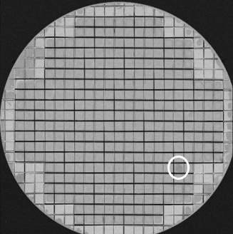
Related Images