Advanced packaging materials
-
Technology Name
Advanced Packaging Material - Wafer Thinning Protective Material(TBDB, Temporary Bonding De-Bonding)
-
Overview
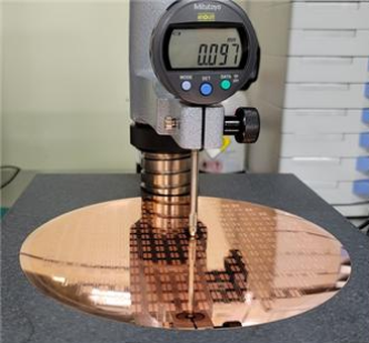
This developed material is a liquid-based wafer backgrinding material and process material. By applying interfacial energy and elasticity coefficient control technology, it completely covers the structures on the front of the wafer with a liquid material before performing the wafer backgrinding process, and solidifies it to eliminate the empty space between the structure and the protective material. This minimizes the concentration of force during subsequent backgrinding, preventing wafer breakage, and applies wafer front passivation (protection) material technology and process technology for high-efficiency wafer backgrinding process for thicknesses of 120 micrometers or less, ensuring thickness uniformity and increasing backgrinding yield and efficiency.
-
Technical Features
Based on the results of preliminary research on liquid-based backgrinding coating material and process compatibility for thinning bare wafers, the 9-step process of carrier film bonding, carrier wafer bonding, backgrinding, delamination, cleaning, dicing tape bonding, dicing, UV exposure, and dicing tape debonding in the wafer backgrinding process protocol using the existing imported front protection carrier film has been simplified to a 6-step process of resin coating, carrier film lamination, UV exposure, backgrinding, dicing, and film delamination for commercialization.
-
Technical Advantages
This developed material, as a liquid-based material for front protection before wafer backgrinding, provides interfacial energy and elasticity coefficient that can show strong resistance to shear stress during wafer backgrinding after solidification, and can show easy heterogeneity when vertically separated from the wafer after backgrinding. This increases the stability, efficiency, and yield of the wafer backgrinding process, while inducing cost and time savings through process simplification.
- Expectations for improved wafer backgrinding stability and yield through strong backgrinding shear stress resistance and easy delamination.
- Expectations for cost and time competitiveness through omission of adhesive residue removal process.
- Competitive advantage over existing products in terms of price.
- Ability to create R&D services to supplement the problems of semiconductor post-processing companies.
-
Application of
TechnologyProduct Application
- The multipurpose carrier film for 2.5D/3D IC semiconductor wafer backgrinding and the pre/post process design for wafer backgrinding can be essential to meet the demand for device wafer thinning, which is becoming essential in semiconductor post-processing.
- The ultimate goal is to reduce the cost of backgrinding tape, laminating tape, dicing tape, etc., which were consumed, and to maximize the stability of the process by improving the low yield and uniformity that occurred in the existing device elements through our new materials and processes, thereby presenting product and application possibilities in various aspects.
- As mentioned above, the results of this technology development, such as the acquisition of coating materials with excellent thermal stability, chemical stability, adhesion and heterogeneity, and the acquisition of coating materials with excellent thickness and uniformity, can be widely used as multipurpose carrier films with high usability in semiconductor production systems.
- By applying to semiconductor packages (Die Level Assy, TSV, Flip chip CSP, High Density & Fine pitch FC, Thin substrate CSP assembly chip, Lead Frame land grid array chip, etc.), it can contribute to the production of more delicate and sophisticated semiconductor products.
- Compatible with Tape Laminating and wafer backgrinding batch process protocol (NNFC).
- It can contribute to the development of high value-added semiconductor technology by linking with 3D IC, D PKG (TSV, WLP) sensors, etc. in-line.
-
Scope of Service and
Technology LevelBackgrinding of device wafers as a post-semiconductor process is essential for thinning required in mobile and small appliances, and through this project, we can secure next-generation domestic technology.
-
Contact Information
Person in charge Park Jae-hongContact 042-366-1731Email jhpark@nnfc.re.kr -
Related Images
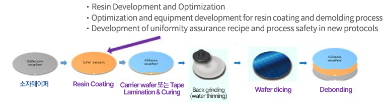
- 소자웨이퍼
- Resin Coating
- Resin 개발 및 최적화
- Resin coating 및 demolding 공정 최적화 및 기구 개발
- 새로운 프로토콜상에서의 공정안전성 확보 및 균일도 호가보 레시피 개발
- Carrier wafer 또는 Tape Lamination & Curing
- Back grinding (water thinning)
- Wafer dicing
- Debonding