Quantum sensor
-
Technology Name
Magnetic Optical Trap Atom Chip for Ultra-small Quantum Sensors
-
Overview
This is a process platform that supports the development of a diffraction grating-based atom chip for capturing and cooling atoms using a single light source.
-
Technical Features
- It is a precise micro-pattern process of silicon for implementing a diffraction grating through DUV-based lithography.
- It is a process that can selectively deposit reflection and dielectric films on the surface of the diffraction grating based on Mix-and-Match lithography using a DUV scanner and I-line exposure equipment.
- It is a dry dicing process that can minimize surface contamination of the magnetic optical trap atom chip through stealth laser dicing.
-
Technical Advantages
- Based on the DUV-based silicon micro-pattern process, it is possible to implement a diffraction grating that can be used up to the short wavelength band. (Minimum linewidth: L/S 70nm)
- Various types of large-diameter atom chips can be produced that can control the laser needed for magnetic optical trapping through 1D or 2D diffraction grating design.
- It has high productivity and price competitiveness with a 200mm large-area silicon process, and it is highly reproducible.
-
Application of
Technology- Computing: It plays a key role in creating neutral atom-based Qbuit for quantum computing.
- Defense/Aerospace: It is also applied to quantum sensors for ultra-precise measurement of time, gravity, magnetic field, inertia, etc.
- Communication: It can be used in the development of quantum light sources and high-sensitivity receivers.
-
Scope of Service and
Technology LevelThe National Nanofab Center has the capability to provide this atom chip process technology for magnetic optical trapping of atoms, and services are possible in the following scope and technology level.
- Support for the development of diffraction grating start products based on 200mm silicon process
- Evaluation of diffraction grating (in preparation)
-
Contact Information
Person in charge Jong Chul ParkContact Number 042-366-1734Email jcpark@nnfc.re.kr -
Related Images
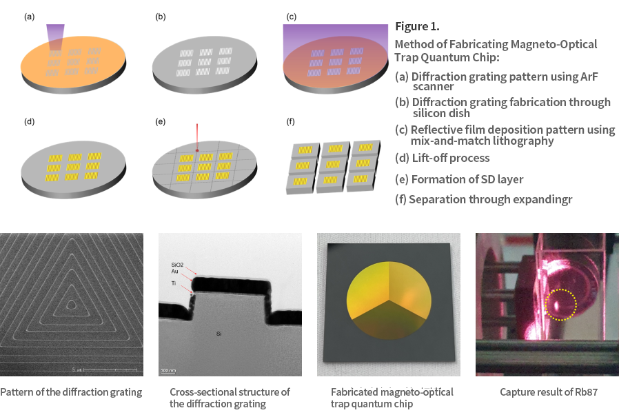 그림 1. 자기광 포획 양자칩 제작 방법
- (a) ArF scanner를 이용한 회절격자 패턴
- (b) 실리콘 식가을 통한 회절격자 제작
- (c) Mix-and-match lithography를 이용한 반사막 증착 패턴
- (d) lift-off 공정
- (e) SD layer 형성
- (f) expanding을 통한 분리
- 회절격자의 패턴
- 회절격자의 단면 구조
- 제작된 자기광 포획 양자칩
- Rb87의 포획 결과
-
Technology Name
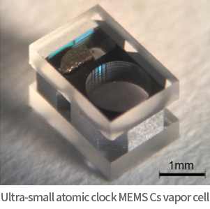
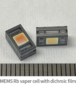
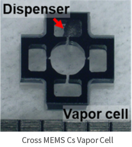
MEMS Alkali Vapor Cell
-
Overview
This is a quantum platform for the development of ultra-small alkali vapor cells, which are at the core of neutral atom-based quantum technology.
-
Technical Features
- This is a manufacturing process for ultra-small alkali vapor cells based on a 200mm silicon process, including Cs and Rb, which are widely used in quantum sensors.
- Through the processing of silicon and glass substrates, it supports the development of MEMS alkali vapor cells with shapes optimized for various quantum devices.
- The MEMS alkali vapor cell includes a dispenser for injecting Cs and Rb, and you can choose N, Ne buffer-gas.
-
Technical Advantages
- This is a vapor cell manufacturing process that can selectively inject Cs and Rb alkali metals into high vacuum or specific pressure buffer-gas.
- This is a vapor cell manufacturing process that can be integrated at the wafer level with various nano films, patterns with diffraction gratings, etc.
- With a 200mm large-area silicon process, it has high productivity and price competitiveness, and excellent reproducibility.
-
Application of
Technology- Computing: It plays a key role in generating neutral atom-based Qbuit for quantum computing.
- Defense/Aerospace: It can also be applied to quantum sensors for ultra-precision measurement of time, gravity, magnetic field, inertia, etc.
- Communication: It can be used for the development of quantum light sources and high-sensitivity receivers.
-
Scope of Service and
Technology LevelThe National Nanofab Center has the capability to provide such atomic vapor cell process technology, and services are possible in the following scope and technology level.
- Support for the development of atomic vapor cell start-up products based on a 200mm silicon process
- Evaluation of vapor cells (in preparation)
-
Contact Information
Person in charge Ye-Eun NaContact Number 042-366-1732Email yeeun.na@nnfc.re.kr -
Related Images