Silicon Photonics
Field
Silicon
Photonics
Photonics
-
Technology Name
Light Source-Optical Device Interface Integration Technology Platform
-
Overview
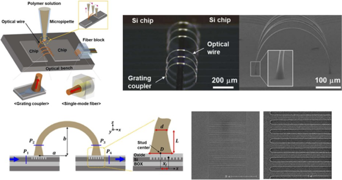
- Silicon photonics technology requires an interface technology to connect an external light source and integrated optical devices, as it cannot provide a light source that generates light.
- This technology provides an integrated technology of optical waveguides and light source couplers on an SOI substrate that provides an optical wire bonding and optical fiber interface for efficient coupling of light sources and optical devices.
-
Technical Features
- Can provide specialized optical device module processes according to the optical properties of integrated optical device materials and the structure of external optical fibers and optical wire bonding.
- Based on FDTD electromagnetic field analysis technology for mode matching between multi-mode external polymer optical waveguides and single-mode integrated optical devices.
-
Technical Advantages
- Provides high-precision lattice coupler integration technology based on 8-inch CMOS compatible process.
- Low-loss optical waveguide integration technology for connecting light source couplers and subsequent optical devices.
-
Application of
the Technology- Quantum integrated circuit fields in quantum communication, computing, and sensor fields.
- Optical transceiver fields such as data centers and 6G in next-generation communication.
- Optical phase array fields for implementing fixed LiDAR-on-chip in advanced mobility.
-
Scope of Service and
Technology LevelTechnology for producing starting products of optical waveguides and lattice couplers required for optical wire bonding and optical fiber coupling.
-
Contact Information
Person in charge Jongbeom YooContact Number 042-366-1606Email jbyou@nnfc.re.kr -
Related Images