2004.05.04
※ Basis of Establishment: Nanotechnology Development Promotion Act (Article 11)
Overview
Overview
Date of establishment
Purpose of establishment
R&D support through joint use of facilities and equipment,
Commercialization of Research Results and Support for Small and Venture Companies
-
Main functions
- Support for joint use and utilization of R&D facilities and equipment related to nanotechnology in industry, academia, and research
- Support for process and application research and development to create new nano-convergence industries
- Training professionals using advanced equipment and facilities
- Commercialization of Research Results and Support for Small and Medium Business Start-ups
-
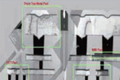
Achievements of Research and Development Support
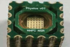
- Joint development of World's smallest 3nm FinFET (Nano Electronic Device) ('06.3)
- Joint development of next-generation fusion memory (U-RAM) ('08.7)
- Joint development of the world's first 3DIC commercialization technology ('08.8)
- Joint development of the world's first 20nm gap integrated nano-device ('09.12)
- Joint development of 50nm Spectroscopic Sensor ('10.12)
-
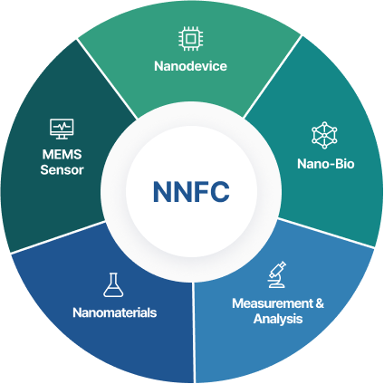
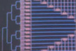
Platform Technology
- CMOS Platform : 0.18um SOI RF
- MEMS Platform : Sa-FPA
(Semi-active Focal Plane Array) - More than Moore Platform : HSoS
(Heterogeneous Systems On Silicon) - NBIT Platform : u-TAS(Micro-Total Analysis System)
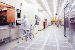
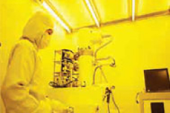
Facilities
-
Clean room5,067㎡(2 stories)
- Class 1 : 605㎡
- Class 100 : 1,355㎡
- Class 10,000 : 1,015㎡
- Others : 2,092㎡
-
Central Utility6,433㎡(9 stories and 1 underground)
-
Office4,620㎡(4 stories and 1 underground)
Main Service Fields
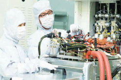
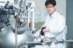
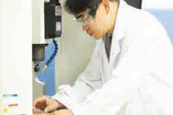
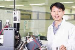
Infrastructure
Cleanroom for
Nano-Device
Nano-Device
E-BEAM, KrF Scanner + etc (Total 50 equipments)
Cleanroom for
NEMS/MEMS-Sensor
NEMS/MEMS-Sensor
Deep Si Etch, Wafer Bonder + etc (Total 55 equipments)
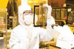
Department of
Nanomaterials
Nanomaterials
Nano Cluster & Generator, Graphene CVD + etc (Total 9 equipments)
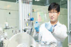
Department of
Nano-Bio
Nano-Bio
SPR, Confocal Microscope + etc (Total 11 equipments)
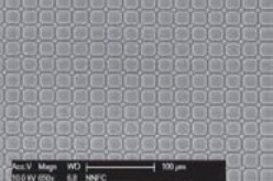
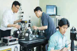
Department of
Measurement and Analysis
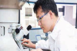
Measurement and Analysis
Cs-corrected STEM, SIMS + etc (Total 41 equipments)