Batch process
Technical Features
Not only does it involve using materials of ultra-thin films relative to the size of the pattern, but it also necessitates the development of new processes that align with the optical properties of transparent and metal electrodes for the display. Therefore, it is a highly challenging technology that must simultaneously satisfy both the electrical properties of semiconductors and the optical properties of displays.
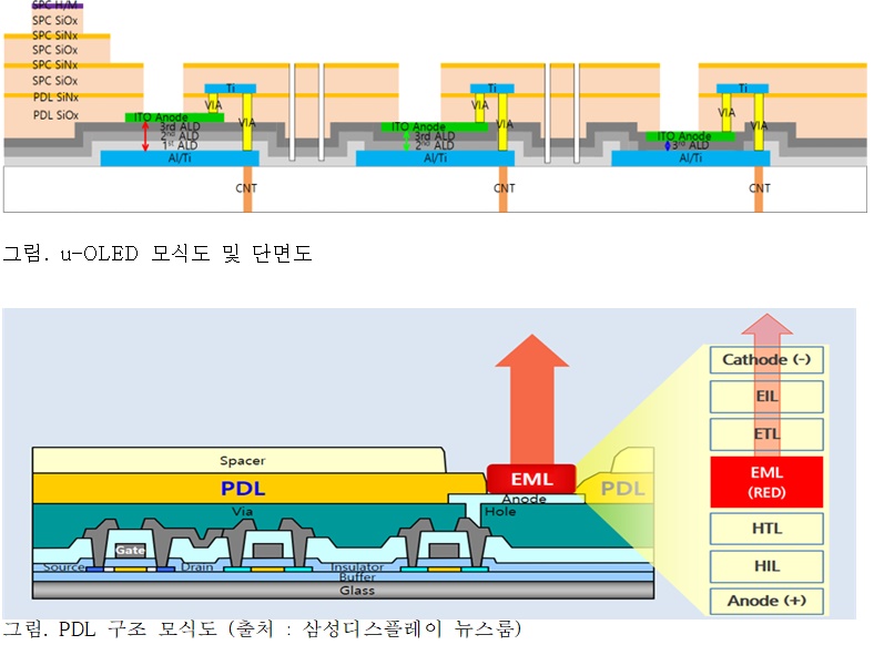
The significance of structure formation and process technology development for PDL (Pixel Defined Layer): PDL (Pixel Define Layer) is a layer in an OLED panel that separates each sub-pixel of the organic light-emitting layer (EML) to prevent interference between them (refer to the figure). In an OLED panel, each RGB sub-pixel, which uses organic light-emitting materials to produce Red, Green, and Blue colors, is created through the Evaporation process. PDL is formed on the areas outside of the deposition area of each sub-pixel before the deposition of the organic light-emitting material takes place.
Experience in developing and completing unit processes and Photo Array necessary for the development of Micro OLED with 4500ppi, low voltage operation, and high brightness.
Experience in developing and completing panel technology.
Secured electrode characteristics specialized in Micro OLEDOS development, including transparent electrodes.
Experience in developing and completing Photo Defined Layer.
Experience in developing and completing PR for Color Filter.
Experience in R & D and completion for μ-LED.
μ-OLEDOS on ROIC wafer.

Public Domain Type 4
- Source indication
- Only non-commercial use possible
- No modification or secondary works allowed
If you wish to use materials that do not have the public domain attached, please use them after prior consultation with the person in charge of the NATIONAL NANOFAB CENTER website.