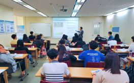
Program details
Nano-specialist Training and Job Support Program
A program to train nano-specialists through on-site internships for unemployed graduates (or expected graduates) in the field of engineering.
Recruitment target: Unemployed graduates (including expected graduates) in the field of engineering
Selection method
-
STEP.01 Recruitment announcement
-
STEP.02 Document screening
(1st round) -
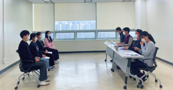
STEP.03 Interview
(2nd round) -
STEP.04 Announcement of successful candidates
Recruitment schedule and procedure
| Round | Announcement | Document/Interview Evaluation | Announcement of successful candidates | Start of training |
|---|---|---|---|---|
| 1st round (25 people) | Early January | End of January | Early February | Mid-February |
| 2nd round (25 people) | End of March | Mid-April | Mid-April | Early May |
| 3rd round (25 people) | End of May | Mid-June | End of June | Early July |
| 4th round (25 people) | Early August | Mid-August | Early September | Mid-September |
The above schedule is subject to change based on the year 2024.
Training benefits
Full tuition waiver (theory/practical training)
Monthly training support: 500,000 KRW per month
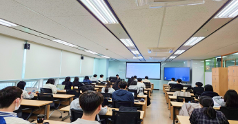
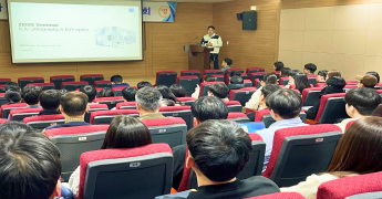
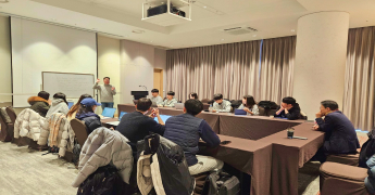
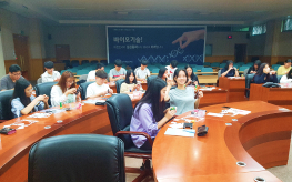
Job competency enhancement workshop
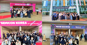
Company recruitment briefing session
Award for excellent presentation on semiconductor device fabrication
Training stages
- Semiconductor industry trends
- Theory of 8 major semiconductor processes and devices
- Theory of semiconductor post-processing and analysis
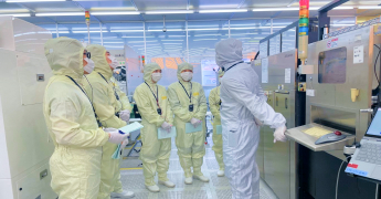
- Group on-site training on semiconductor process equipment
- Acquisition of basic knowledge of equipment by process
- Understanding of FAB process duties and business process
- Setting of project topic and practical training
- Evaluation of equipment operation and key parameters
- Acquisition of key management items by equipment
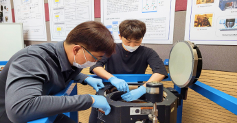
- Equipment disassembly and assembly
- Theory and discussion of semiconductor devices
- Fab Process and process progress
- Fabrication and measurement analysis of semiconductor MOS Cap. /MM Cap. devices
- PT presentation and evaluation
The training curriculum may change depending on the operation of the training.
Heo Kang (042-366-1530), Ryu Hana (042-366-2094)
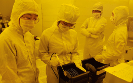
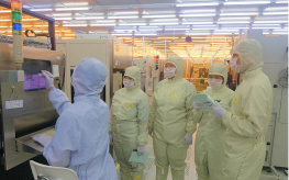
Training of specialized personnel for nano-infrastructure utilization
(practical training for silicon-based nano-device process and measurement analysis)
Recruitment target: Unemployed graduates (including expected graduates) in the field of engineering
Recruitment schedule and procedure
| Training | Training course | Number of trainees | Training period |
|---|---|---|---|
| Foundation | Nano-deviceㆍprocess | 18 | 23. 5. 15. ~ 23. 5. 19. |
| Foundation | Nano-analysis evaluation | 15 | 23. 5. 22. ~ 23. 5. 26. |
| Specialization | GOI manufacturing technology | 15 | 23. 11. 20. ~ 23. 11. 24. |
| Specialization | Equipment specialized training | 10 | 23 1. 5. ~ 23. 1. 12. |
| Comprehensive practical | Measurement analysis (summer) | 25 | 23. 7. 3. ~ 23. 8. 25. |
| Comprehensive practical | Device process (winter) | 30 | 23. 12. 18. ~ 24. 2. 8. |
Short-term course (basic/application): Selected from those who have completed the theoretical training of the Nano Technology Research Council
Long-term course (advanced): Selected by the institute itself (document screening + interview)
Training benefits
Full tuition waiver (theory/practical training)
Operation system focused on on-site practical training
Company recruitment briefing session
Job mentoring by professional committee
Award for excellent trainees (10 people/year) with certificate of commendation (Minister's Award) and gifts
Accommodation fee (within a certain limit) support
Lunch provided
Training course
content 을 기준으로 각 교육과정을 설명합니다.
- 5 days / 1 session
- 18 people
- Strengthening practical training centered on the use of process equipment linked to the nano-device process theory training course
- 5 days / 1 session
- 15 people
- Strengthening practical training centered on the use of analysis equipment linked to the nano-analysis evaluation theory training course
- 5 days / 1 session
- 15 people
- GOI device structure fabrication and characteristic interpretation capability strengthening practical training
- 1 day / 3 sessions
- 10 people
- Advanced training on research equipment centered on the demand of graduate students in the field of engineering to enhance research and development capabilities
- 8 weeks / 1 session
- 25 people
- Strengthening practical skills in semiconductor measurement and analysis with a focus on employment linkage with nano-convergence companies
- 8 weeks / 1 session
- 30 people
- Strengthening job capabilities in semiconductor process and device fabrication with a focus on employment linkage with advanced industries
87.5% of the graduates in '21 have completed employment
| 2024 training plan | ||||||||||||||
|---|---|---|---|---|---|---|---|---|---|---|---|---|---|---|
| Implementation content | Number of trainees | Training schedule | Implementation schedule | |||||||||||
| 1 | 2 | 3 | 4 | 5 | 6 | 7 | 8 | 9 | 10 | 11 | 12 | |||
| Nano device process practical training | 15 people | 2 months(07.01 ~ 08.24) | Have training | Have training | ||||||||||
The schedule may change depending on the status of the institution in the future.
Baek Jong-hoon (042-366-2091), Yu Ji-young (042-366-2096)
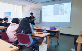
Specialized High School Nano-Convergence Technology Education (Job Creation)
On-site customized education for semiconductor duties (Maintenance, Operator) targeting 3rd year students in specialized high schools in Daejeon Metropolitan City
Recruitment target: 3rd year students in specialized high schools in Daejeon Metropolitan City
Recruitment schedule and quota: (planned) April~May, within 40 people
Training schedule: (planned) September ~ December
Training content
Training curriculum (over 450 hours)
-
Theory training(3 weeks)
Major theory
- Basic terms of nanotechnology
- Basics of nano-semiconductors
- Theory of semiconductor process
- Theory of package technology
- Industry-specific courses
- Ethics education
- Cultivation education
-
Basic practical training(3 weeks)
- Group equipment process experience and learning of equipment roles
- 8 field rotation practical training (photolithography, etching, diffusion, thin film, characteristic analysis, new materials, bio, equipment disassembly practical training)
-
Maintenance practical training(1 weeks)
- Semiconductor chamber disassembly, assembly
- Recipe Tunning
- Understanding the function of major semiconductor parts
- Equipment Trouble-shooting
- Equipment parts fabrication practical training
-
Advanced practical training(2 months)
- 1:1 mentoring system
- Learning and evaluation of equipment operation capabilities
-
Industry on-site practical training
- Package industry on-site practical training
- Experience of the entire semiconductor process
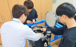
Training site photos
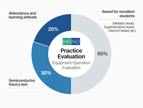
Trainee evaluation system
Training benefits
Full tuition waiver (theory/practical training)
Monthly training support of 250,000 KRW, lunch provided
Semiconductor company recruitment briefing session and semiconductor exhibition attendance
Award for excellent trainees: Minister of Trade, Industry and Energy Award, Director of National Nanofab Center Award
Selection of excellent/improved trainees every month: Gift worth 50,000 KRW
Main employment destinations ('23 employment rate 94%)
Lee Kwang-chul (042-366-2095), Lee Yoon-ji (042-366-2092)
Open Equipment Training
Open Equipment Training Overview
"Equipment Training" is conducted for users who want to directly use the shared equipment of the institute in accordance with the "Guidelines for Open Use and Direct Use Management of Owned Equipment (2021.03.18.)" established to expand the use of Nanofab facilities and shared equipment.
Recruitment target: Employees, students, researchers
Application period: Beginning of each month
Application method: Moaform application
Training equipment and training quota
| Training content | Training hours | Training fee (KRW) | Training quota | Minimum number of people | Researcher in charge | Remarks |
|---|---|---|---|---|---|---|
| PR Stripper | 13:30~16:30 | 300,000 | 3 | 2 | Researcher Jo Hee-jae | |
| Furnace | 13:30~16:30 | 300,000 | 3 | 2 | Senior Hwang Hae-chul | |
| Blade Dicer | 13:30~16:30 | 200,000 | 3 | 1 | Researcher Kim Su-hyun | |
| 2D Profiler | 13:30~16:30 | 200,000 | 3 | 1 | Senior Son Woo-sik | |
| FE-SEM | 13:30~16:30 | 200,000 | 3 | 1 | Manager Hyun Moon-seop | |
| Back-Grinder | 13:30~16:30 | 200,000 | 3 | 1 | Senior Kim Tae-hyun | |
| Paticle Size Analyzer | 13:30~14:30 | Free | 5 | 1 | Senior Lee Yong-hee | * Characteristics of this equipment
|